
TM 11-6625-2575-14
SWEEP RATE -------------- LINE.
and waveforms are shown which are typical of
RF VERNIER ----------- Set to 0.5 volts rms into a
an operating AN/USM-203A. In addition, a trou-
50-ohm load.
bleshooting guide is presented in table 7-2 which
ALC-------------------------- INT.
lists symptoms, probable causes, and recommend-
MARKERS ------------ ON (1.0, 10.0, and 50 MHz).
ed corrective actions.
FIXED MARKER SIZE --- Midrange.
NOTE
CAUTION
Troubleshooting and repair of rf assem-
In making measurements, the chassis of
blies shall be performed at higher main-
the AN/USM-203A shall be connected to
tenance categories.
the chassis or ground connection of the
test instrument.
and 7-11. The dc voltage measurements are made
forms in figures 7-2 through 7-8 are typical of
those in a normal AN/USM-203A when the unit
the voltmeter probe shall be common to the AN/
is connected to a 115-volt ac line, the POWER
USM-203A chassis. The waveform measurements
are made. with a de-coupled, high-impedance os-
switch is at ON, and a 20-minute warmup is used.
Other front panel controls and the internal blank-
cilloscope probe at the test point. The probe
ing switch are set as follows:
shield is common to the AN/USM-203A chassis.
The waveforms (fig. 7-2 through 7-8) displayed
BAND
---------------- HIGH.
on the oscilloscope are typical for the AN/USM-
ATTENUATOR ------------- 0 dB.
BLANKING
----- VIDEO (main PC board).
203A. Variation from the typical voltages or
SWEEP WIDTH ---------- WIDE.
waveshapes should be carefully noted during trou-
SWEEP WIDTH vernier --- Fully clockwise.
bleshooting.
CENTER FREQUENCY --- 1000 MHz.
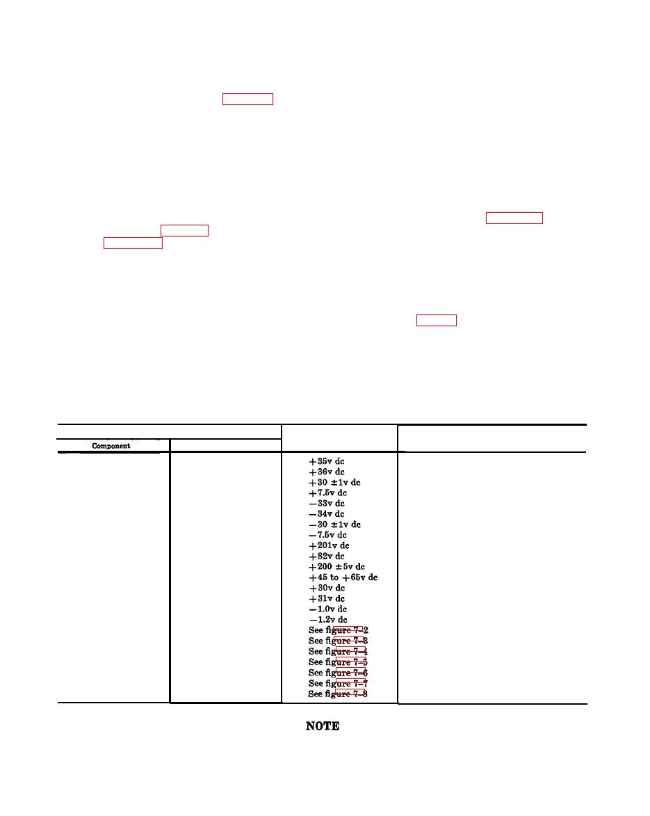
Test Point
Voltage
(Test point to mound)
Terminal
Function
Emitter
Q3
Q1 base drive voltage
Cathode
Q3 base drive voltage
VR2
Anode
+ 30v dc regulated output
VR2
Cathode
VR3
Reference voltage for +30v dc
Emitter
Q7
Q5 base drive voltage
Anode
Q7 base drive voltage
VR5
Cathode
VR5
- 30v dc regulated output
Anode
VR6
Reference voltage for - 30v dc
Emitter
Q1O
Q9 base drive voltage
Emitter
Q11
Q10 base drive voltage
Anode
VR7
+ 200v dc regulated output
Positive
C2
+ 50v dc Supply
Emitter
Q201
Leveled B+ voltage
Collector
Q202
Q201 base drive voltage
Base
Q206
Leveler sample voltage
Base
Q207
Leveler reference voltage
Q102
Collector
Schmitt trigger output
Emitter
Q105
Emitter follower
Q106
Collector
Linear amplifier output
Q107
Collector
Nonlinear amplifier
4
J301
Output of LO-MHZ marker
J302/J303
4
Output of 10.0- and 50-MHz markers
Q305
Collector
Output of first stage of marker amplifier.
All voltages indicated in column 3 are typical, except where a specific tolerance or
range is given.

