TM11-6625-2948-14+P
d. EXT
Position. In the EXT
position, the
THE +40V (-1280V) REF GROUND POWER
input to the Schmitt trigger gate is placed at ground poten-
SUPPLIES
tial (-1280V) so that initially the klystron tube does not
conduct. The input to the Schmitt trigger, however, is
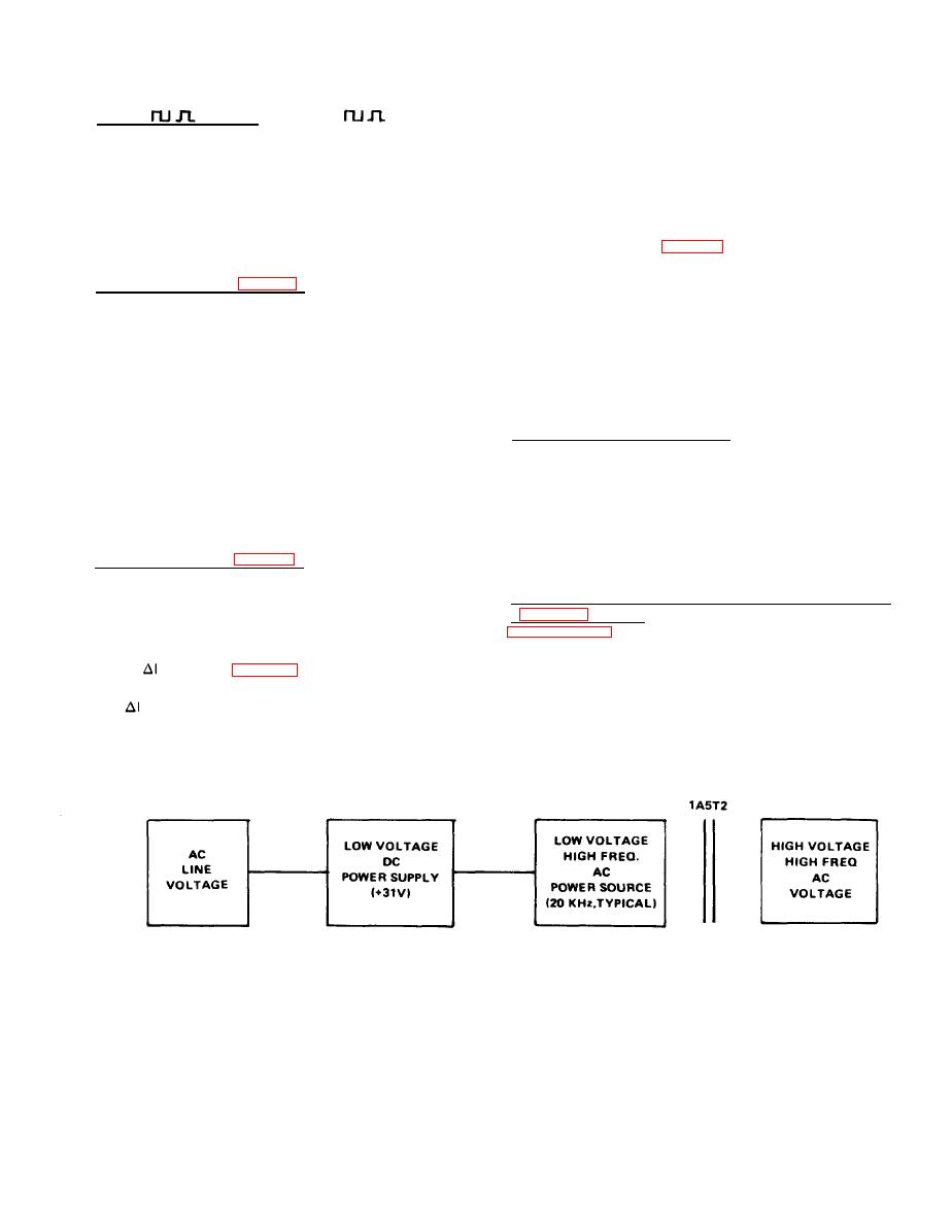
The power supplies used for the generation of beam,
driven by positive going pulses from an external source
repeller and control circuits are not conventional. A block
a p p l i e d at the EXT MOD connector 1J3. The klystron
d i a g r a m of the processes by which high voltages are
tube conducts only during that portion of the cycle when
generated is shown in Fig. 3-2. A low voltage dc power
the pulse fs on.
supply (+31V) is derived from the ac line voltage using a
e. INT FM ~ Position (Fig. 2-2). In the INT FM ~ position
conventional, step-down transformer 1A2T1, bridge
rectifier, and filter networks for low ripple. It supplies the
the Schmitt trigger is biased so that the output of the
main current for subsequent conversion to a high voltage
amplifier is at +40V; thus, the grid is at a potential so
ac generator. The dc voltage is converted to o low voltage
t h a t oscillations in the klystron tube takes place. The
h i g h frequency, ac power source (20 KHz, typical) by
voltage on the repeller electrode of the tube is modulated
oscillator 1A5Q1 and 1A5Q2. The low ac voltage is stepped
by a sine wave voltage as derived from the line voltage
up to suitable ac voltages by transformer 1A5T2.
through transformer 1A2T1. The FM deviation is deter-
mined by resistor 1A3R16 and the rate is fixed at the line
a. Low Voltage DC Power Supply. The main ac line voltage
frequency. In addition, a horizontal sweep output is avail-
stepped
down to approximately 31 vac and rectified
able at connector 1J1 whose phase can be varied by HOR
IS
using bridge rectifier 1A4BR1. The rectified voltage is
SWP PHASE control resistor 1A3R4. With the use of the
filtered and the ripple is kept low using Darlington capaci-
HOR SWP OUT and PHASE controls, the rf output modu-
tor multiplier 1A4Q4 and 1A4Q5. Capacitor 1A4C1
lation can be viewed on an oscilloscope with the aid of an
provides the fundamental filtering. The effective capaci-
RF detector.
tance of 1A4C2 is increased by the current gains of 1A4Q4
f. EXT FM Position (Fig. 2-2). In the EXT FM position,
and 1A4Q5.
he oscillations take place as described in the INT FM ~
b. Low Voltage High Frequency AC Voltage Generator
position. The repeller voltage is modulated by the external
voltage applied at connector 1J2.
f r e q u e n c y as follows. Two PNP transistors 1A5Q1 and
F CONTROL (Fig. 2-2)
1A5Q2,
and
transformer
1A5T1
comprise
the
basic
oscil-
lator. The emitter is connected to the +31V dc line through
the current limiter 1A4Q1. The bias voltage to the bases
F control varies the repeller voltage over a relatively
The
is determined by the collector voltage of transistor 1A4Q3.
small range to provide a frequency vernier adjustment.
ELSYQ-7


