TM 11-6625-3041-30/TO 33A1-8-908-12
1-15. RECEIVE 1 (A5) NRZ IN (CONT)
The balanced timing signal is applied to the front panel
BAL
BALANCED TMG IN connector and to an amplifier. A O-level 04
TMG IN
and a O-level 05 output from Decode II enable the amplifier
only for the 128-4608 family DATA RATES (balanced NRZ).
The output of the
Bal
BAL TMG IN amplifier
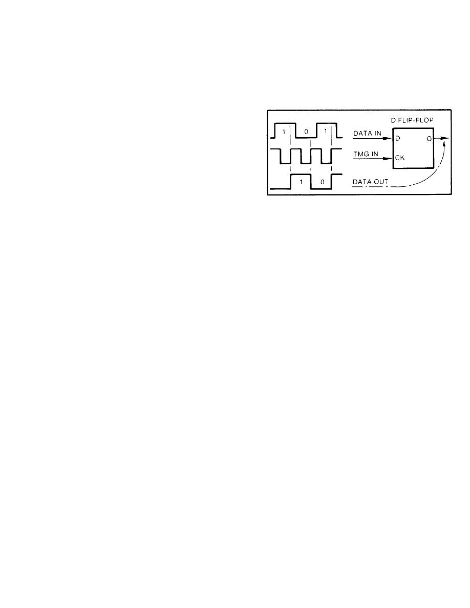
Data Retime
is applied to the D
input of the Bal
Data Retime, a D
flip-flop.
The clock input to
the flip-flop is the
balanced timing sig-
nal . It is used to clock the data out of the flip-flop (in
the same manner as the Unbal Data Retime above) to ensure the
data input is in phase with the timing input.
The outputs from the Unbal Data Retime and Bal Data Retime
Data
are applied to the input of the Data Fam Sel. A third input
Fam Sel
is derived from the diphase signal.
One of the inputs is selected as the output, depending on the
setting of the DATA RATE control (through the 04 and 05 outputs
from Decode II). For example, a Decode 11 output of 00 selects
the 128-4608 family (balanced NRZ) as the output.
The output from the UNBAL TMG IN amplifier and BAL TMG IN
Clock
amplifier are applied to the input of the Clock Fam Sel. A
Fam Sel
third input is derived from the diphase signal.
One of the inputs is selected as the output, depending on the
setting of the DATA RATE control (through the 04 and 05 outputs
from Decode II). For example, a Decode II output of 00 selects
the 128-4608 family (balanced NRZ) as the output.
The output from the Clock Fam Sel is applied to the input of
NRZ/Diphase
the NRZ/Diphase Clock Sel. A second input is derived from the
Clock Sel
diphase signal.
One of the inputs is selected as the output, depending on the
setting of the DATA RATE control (through the 04 output from
Decode II). For example, a Decode II output of O selects
the 576 ATACS or 128-4608 family (NRZ) as the output.
1-13


